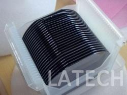
Epi-ready single crystal Ge wafer
| Product: | Germanium (Ge) wafer |
| Purity: | 99.9999% (6N) |
| Material property: | Crystal structure: cubic |
| Lattice constant: a = 5.6576 Å | |
| Bandgap: 0.67 eV (300 K) | |
| Melting point: 937.4 °C | |
| Dimension: | • 2'' × 0.4 mm, 2'' × 0.5 mm • 4'' × 0.5 mm • Other dimensions available |
| Orientation: | <100> / <110> / <111> / others |
| Conductive type: | Undoped native / n-type / p-type |
| Resistivity: | • 1 - 50 Ω·cm for undoped native wafer (exhibiting n-type behavior) • 0.01 - 0.07 Ω·cm for n-type and p-type doped wafers |
| Etch pit density (EPD): | • Low 1000 - 5000 cm-2 • High < 10000 cm-2 |
| Polishing: | Single side / double side epi-polished |
| Surface roughness: | < 0.5 nm |